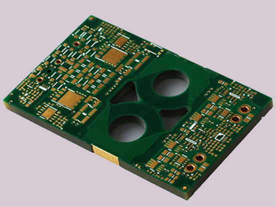
Thick copper circuit board
Introduction of Thick Copper Circuit Board Technology
(1)Pre-plating preparation and electroplating treatment
The main purpose of thickening copper plating is to ensure that there is a thick enough copper plating layer in the hole to ensure that the resistance value is within the range required by the process. As a plug-in, it is to fix the position and ensure the connection strength; as a surface-mounted device, some holes are only used as through holes, which play the role of conducting electricity on both sides.
(2)Inspection items
1. Mainly check the metallization quality of the hole, and ensure that there is no excess, burr, black hole, hole, etc. in the hole;
2. Check whether there is dirt and other excesses on the surface of the substrate;
3. Check the number, drawing number, process document and process description of the substrate;
4. Find out the mounting position, mounting requirements and the coating area that the plating tank can bear;
5. The plating area and process parameters should be clear to ensure the stability and feasibility of the electroplating process parameters;
6. Cleaning and preparation of conductive parts, first electrification treatment to make the solution active;
7. Determine whether the composition of the bath liquid is qualified and the surface area of the electrode plate; if the spherical anode is installed in the column, the consumption must also be checked;
8. Check the firmness of the contact parts and the fluctuation range of voltage and current.
(3)Quality control of thickened copper plating
1. Accurately calculate the plating area and refer to the influence of the actual production process on the current, correctly determine the required value of the current, master the change of the current in the electroplating process, and ensure the stability of the electroplating process parameters;
2. Before electroplating, first use the debugging board for trial plating, so that the bath is in an active state;
3. Determine the flow direction of the total current, and then determine the order of the hanging plates. In principle, it should be used from far to near; to ensure the uniformity of the current distribution on any surface;
4. To ensure the uniformity of the coating in the hole and the consistency of the thickness of the coating, in addition to the technological measures of stirring and filtering, it is also necessary to use impulse current;
5. Regularly monitor the changes of the current during the electroplating process to ensure the reliability and stability of the current value;
6. Check whether the thickness of the copper plating layer of the hole meets the technical requirements.
(4)Copper plating process
In the process of thickening copper plating, the process parameters must be regularly monitored, and unnecessary losses are often caused due to subjective and objective reasons. To do a good job of thickening the copper plating process, the following aspects must be done:
1. According to the area value calculated by the computer, combined with the experience constant accumulated in the actual production, increase a certain value;
2. According to the calculated current value, in order to ensure the integrity of the plating layer in the hole, it is necessary to increase a certain value, that is, the inrush current, on the original current value, and then return to the original value within a short period of time;
3. When the electroplating of the circuit board reaches 5 minutes, take out the substrate to observe whether the copper layer on the surface and the inner wall of the hole is complete, and it is better that all the holes have a metallic luster;
4. A certain distance must be maintained between the substrate and the substrate;
5. When the thickened copper plating reaches the required electroplating time, a certain amount of current must be maintained during the removal of the substrate to ensure that the surface and holes of the subsequent substrate will not be blackened or darkened.
Precautions:
1. Check the process documents, read the process requirements and be familiar with the machining blueprint of the substrate;
2. Check the surface of the substrate for scratches, indentations, exposed copper parts, etc.;
3. Carry out trial processing according to the mechanical processing floppy disk, carry out the first pre-inspection, and then process all the workpieces after meeting the technological requirements;
4. Prepare the measuring tools and other tools used to monitor the geometric dimensions of the substrate;
5. According to the raw material properties of the processing substrate, select the appropriate milling tool (milling cutter).
(5) Quality control
1. Strictly implement the first article inspection system to ensure that the product size meets the design requirements;
2. According to the raw materials of the circuit board, reasonably select the milling process parameters;
3. When fixing the position of the circuit board, carefully clamp it to avoid damage to the solder layer and solder mask on the surface of the circuit board;
4. To ensure the consistency of the external dimensions of the substrate, the positional accuracy must be strictly controlled;
5. When disassembling and assembling, special attention should be paid to padding the base layer of the substrate to avoid damage to the coating layer on the surface of the circuit board.