The PCB routing is very important!
When make the PCB routing , due to the preliminary analysis work is not done or not done, the post-processing is difficult. If the PCB board is compared to our city, the components are like row upon row of all kinds of buildings, signal lines are streets and alleys in the city, flyover roundabout island, the emergence of each road is its detailed planning, wiring is also the same.
1. Wiring priority requirements
A) Key signal lines are preferred: power supply, analog small signal, high-speed signal, clock signal, synchronization signal and other key signals are preferred.
B) Wiring density priority principle: Start wiring from the component with the most complex connection relationship on the board. Cabling starts from the most densely connected area on the board.
C) Precautions for key signal processing: try to provide special wiring layer for key signals such as clock signal, high-frequency signal and sensitive signal, and ensure the minimum loop area. If necessary, shielding and increasing the safety spacing should be adopted. Ensure signal quality.
D) The network with impedance control requirements shall be arranged on the impedance control layer, and its signal cross-division shall be avoided.
2. Wiring scrambler control
A) Interpretation of the 3W principle
The distance between the lines should be 3 times the line width. In order to reduce crosstalk between lines, the line spacing should be large enough. If the line center distance is not less than 3 times the line width, 70% of the electric field between lines can be kept without interference, which is called the 3W rule.
B) Tampering control: CrossTalk refers to the mutual interference between different networks on PCB caused by long parallel wiring, mainly due to the action of distributed capacitance and distributed inductance between parallel lines. The main measures to overcome crosstalk are:
I. Increase the spacing of parallel cabling and follow the 3W rule;
Ii. Insert ground isolation cables between parallel cables
Iii. Reduce the distance between the cabling layer and the ground plane.
3. General rules for wiring requirements
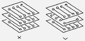
A) The direction of the adjacent plane is orthogonal. Avoid the different signal lines in the adjacent layer in the same direction to reduce unnecessary inter-layer tampering; If this situation is difficult to avoid due to board structure limitations (such as some backplanes), especially when the signal rate is high, you should consider isolating wiring layers on the ground plane and signal cables on the ground.
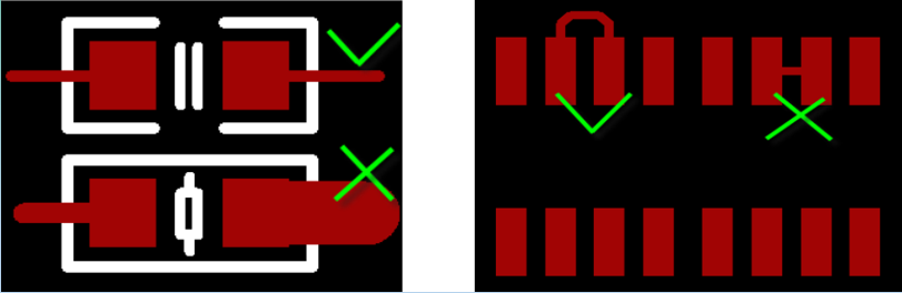
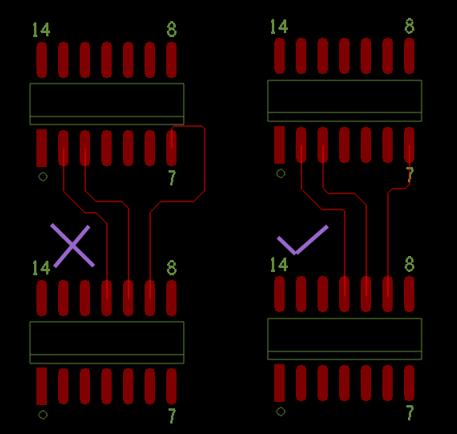
B) The wiring of small discrete devices must be symmetric, and the SMT pad leads with relatively close spacing should be connected from the outside of the pad. Direct connection in the middle of the pad is not allowed.
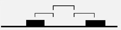
C) Minimum loop rule, that is, the area of the loop formed by the signal line and its loop should be as small as possible. The smaller the area of the loop, the less the external radiation and the smaller the external interference.
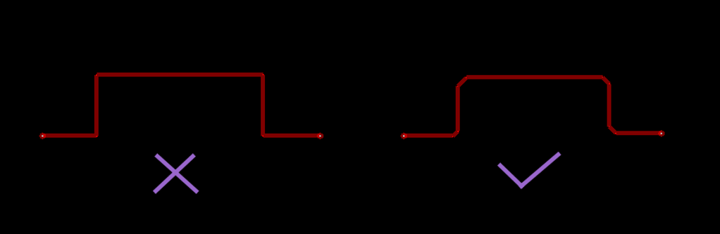
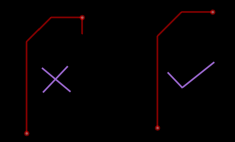
D) STUB cables are not allowed
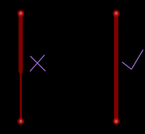
E) The wiring width of the same network should be kept the same. The variation of the wiring width will cause the uneven characteristic impedance of the line. When the transmission speed is high, reflection will occur. Under some conditions, such as the connector lead wire, BGA package lead wire similar structure, because of the small spacing may not be able to avoid the change of line width, should try to reduce the effective length of the middle inconsistent part.
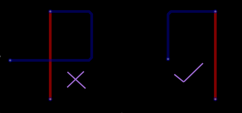
F) Prevent signal cables from forming self-loops between different layers. This kind of problem is easy to occur in the design of multilayer plates, and the self-loop will cause radiation interference.
G) Acute Angle and right Angle should be avoided in PCB design, resulting in unnecessary radiation, and the production process performance of PCB is not good.