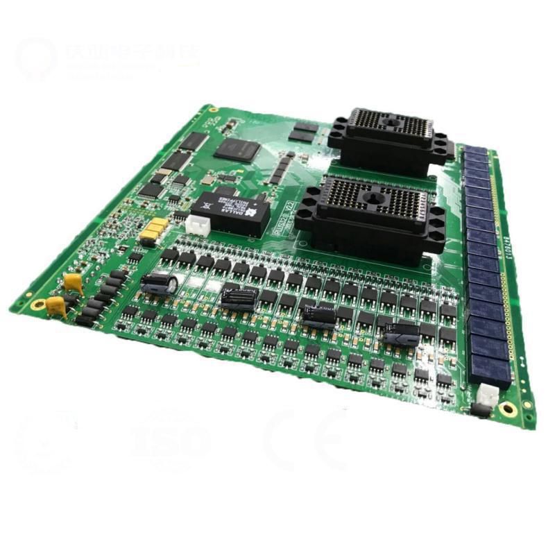
Introduction to reliability testing of PCB circuit boards
The PCB circuit board can combine many electronic components together, which can save space very well and will not hinder the operation of the circuit. There are many processes in the design of the PCB circuit board. First, we need to set Check the parameters of the PCB circuit board. Second, we need to fit the various parts in their proper positions.
1. Enter the PCB design system and set the relevant parameters
Set the environmental parameters of the design system according to personal habits, such as the size and type of the grid point, the size and type of the cursor, etc. Generally speaking, the default value of the system can be used. In addition, parameters such as the size and number of layers of the circuit board must be set.
2. Generate the imported network table
The network table is the bridge and link between the circuit schematic design and the printed circuit board design, which is very important. The netlist can be generated from the circuit schematic diagram, or can be extracted from the existing printed circuit board file. When the network table is introduced, it is necessary to check and correct the errors in the circuit schematic design.
3. Arrange the location of each part package
The automatic layout function of the system can be used, but the automatic layout function is not perfect, and it is necessary to manually adjust the position of each component package.
4. Carry out circuit board wiring
The premise of automatic circuit board routing is to set the safety distance, wire form and other content. At present, the automatic wiring function of the equipment is relatively complete, and the general circuit diagram can be routed; but the layout of some lines is not satisfactory, and the wiring can also be done manually.
5. Save by printer output or hard copy
After completing the wiring of the circuit board, save the completed circuit diagram file, and then use various graphic output devices, such as printers or plotters, to output the wiring diagram of the circuit board.
Electromagnetic compatibility refers to the ability of electronic equipment to work harmoniously and effectively in various electromagnetic environments. The purpose is to enable electronic equipment to suppress various external interferences, enable electronic equipment to work normally in a specific electromagnetic environment, and at the same time reduce the electromagnetic interference of electronic equipment itself to other electronic equipment. As a provider of electrical connections for electronic components, what is the compatibility design of the PCB circuit board?
1. Choose a reasonable wire width. Since the impact interference generated by the transient current on the printed lines of the PCB circuit board is mainly caused by the inductance component of the printed wire, the inductance of the printed wire should be minimized.
2. According to the complexity of the circuit, reasonable selection of the PCB layer number can effectively reduce electromagnetic interference, greatly reduce the PCB volume and the length of the current loop and branch wiring, and greatly reduce the cross-interference between signals.
3. Adopting the correct wiring strategy and using equal wiring can reduce the inductance of the wires, but the mutual inductance and distributed capacitance between the wires will increase. If the layout permits, it is best to use a well-shaped mesh wiring structure. The specific method is to make one side of the printed board horizontal Wiring, wiring on the other side vertically, and then connecting with metallized holes at the cross holes.
4. In order to suppress the crosstalk between the wires of the PCB circuit board, try to avoid long-distance equal wiring when designing the wiring, and keep the distance between the wires as far as possible. cross. Setting a grounded printed line between some signal lines that are very sensitive to interference can effectively suppress crosstalk
