How to place capacitors in PCB design?
Capacitors play an important role in high-speed PCB design and are often the most used device on PCBS. In PCB, capacitors are usually divided into filter capacitors, decoupling capacitors, energy storage capacitors, etc.
1.Power output capacitor, filter capacitor
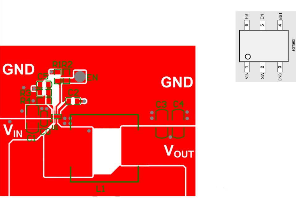
We usually refer to the capacitor of the input and output circuits of the power module as the filter capacitor. Simple understanding is that the capacitor ensures the stability of the input and output power supply. In the power module, the filter capacitor should be large before small. As shown in picture, the filter capacitor is placed large and then small in the arrow direction.
When designing the power supply, it should be noted that the wiring and copper skin are wide enough and the number of holes is sufficient to ensure that the flow capacity meets the demand. The width and number of holes are evaluated in conjunction with the current.
Power input capacitance
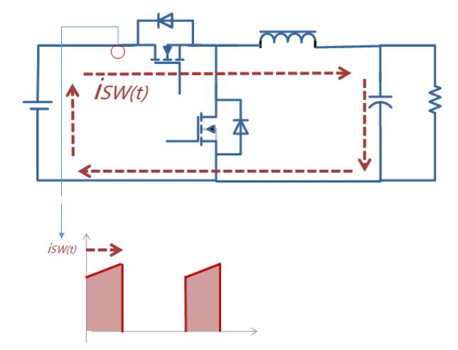
The power input capacitor forms a current loop with the switching loop. This current loop varies by a large amplitude, Iout amplitude. The frequency is the switching frequency. During the switching process of the DCDC chip, the current generated by this current loop changes, including faster di/dt.
In the synchronous BUCK mode, the continuous current path should pass through the GND pin of the chip, and the input capacitor should be connected between the GND and Vin of the chip, so the path may be short and thick.
The area of this current ring is small enough, the better the external radiation of this current ring will be.
2.Decoupling capacitor
The power pin of a high-speed IC needs enough decoupling capacitors, preferably one per pin. In the actual design, if there is no space for the decoupling capacitor, it can be deleted as appropriate.
The decoupling capacitance of the IC power supply pin is usually small, such as 0.1μF, 0.01μF, etc. The corresponding package is also relatively small, such as 0402 package, 0603 package and so on. When placing decoupling capacitors, the following points should be noted.
(1)Place as close as possible to the power supply pin, otherwise it may not have a decoupling effect. Theoretically, the capacitor has a certain decoupling radius, so the principle of proximity should be strictly implemented.
(2)The decoupling capacitor to the power supply pin lead should be as short as possible, and the lead should be thick, usually the line width is 8 ~ 15mil (1mil = 0.0254mm). The purpose of thickening is to reduce lead inductance and ensure power supply performance.
(3)After the power supply and ground pins of the decoupling capacitor are led out of the welding pad, punch holes nearby and connect to the power supply and ground plane. The lead should also be thickened, and the hole should be as large as possible. If a hole with a aperture of 10mil can be used, an 8mil hole should not be used.
(4)Ensure that the decoupling loop is as small as possible
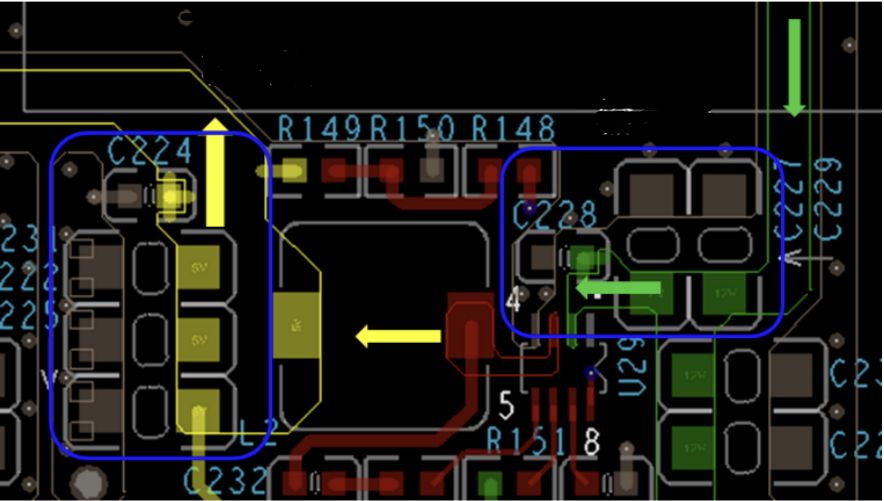
3.Energy storage capacitor
The role of the energy storage capacitor is to ensure that the IC can provide power in the shortest time when using electricity. The capacity of the energy storage capacitor is generally large, and the corresponding package is also large. In the PCB, the energy storage capacitor can be far away from the device, but not too far, as shown in picture. The common energy storage capacitor fan-hole mode is shown in picture.
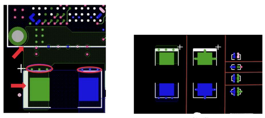
The principles of fan holes and cables are as follows:
(1)The lead is as short and thick as possible, so that there is a small parasitic inductance.
(2)For energy storage capacitors, or devices with large overcurrent, punch as many holes as possible.
(3)Of course, the best electrical performance of the fan hole is the disc hole. The reality needs comprehensive consideration