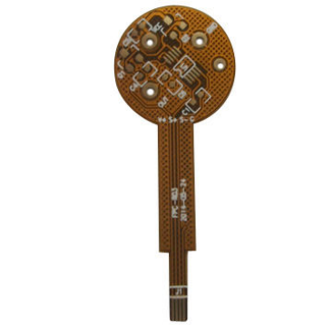
Flexible circuit board welding method steps
1. Before welding, apply flux on the pad and treat it with a soldering iron to prevent the pad from being poorly tinned or oxidized, causing difficulty in soldering. Generally, the chip does not need to be treated.
2. Use tweezers to carefully place the PQFP chip on the PCB board, being careful not to damage the pins. Align it with the pads and make sure the chip is placed in the correct direction. Adjust the temperature of the soldering iron to more than 300 degrees Celsius, dip the tip of the soldering iron with a small amount of solder, use a tool to press down on the aligned chip, and add a small amount of flux to the two diagonal pins, still Press down on the chip and solder the two diagonally positioned pins so that the chip is fixed and cannot move. After soldering the opposite corners, recheck the chip’s position for alignment. If necessary, it can be adjusted or removed and re-aligned on the PCB board.
3. When starting to solder all the pins, add solder to the tip of the soldering iron and coat all the pins with flux to keep the pins moist. Touch the tip of the soldering iron to the end of each pin on the chip until you see the solder flowing into the pin. When welding, keep the tip of the soldering iron parallel to the pin being soldered to prevent overlap due to excessive soldering.
4. After soldering all the pins, soak all the pins with flux to clean the solder. Wipe off excess solder where needed to eliminate any shorts and overlaps. Finally, use tweezers to check whether there is any false soldering. After the inspection is completed, remove the flux from the circuit board. Dip a hard-bristle brush in alcohol and wipe it carefully along the direction of the pins until the flux disappears.
5. SMD resistor-capacitor components are relatively easy to solder. You can first put tin on a solder joint, then put one end of the component, use tweezers to clamp the component, and after soldering one end, check whether it is placed correctly; If it is aligned, weld the other end.
In terms of layout, when the size of the circuit board is too large, although the welding is easier to control, the printed lines will be longer, the impedance will increase, the anti-noise ability will decrease, and the cost will increase; if it is too small, the heat dissipation will decrease, the welding will be difficult to control, and adjacent lines will easily appear. Mutual interference, such as electromagnetic interference from circuit boards. Therefore, PCB board design must be optimized:
(1) Shorten the connections between high-frequency components and reduce EMI interference.
(2) Components with heavy weight (such as more than 20g) should be fixed with brackets and then welded.
(3) Heat dissipation issues should be considered for heating components to prevent defects and rework due to large ΔT on the component surface. Thermal sensitive components should be kept away from heat sources.
(4) The components should be arranged as parallel as possible, which is not only beautiful but also easy to weld, and is suitable for mass production. The circuit board is designed to be a 4:3 rectangle (preferable). Do not have sudden changes in wire width to avoid wiring discontinuities. When the circuit board is heated for a long time, the copper foil is easy to expand and fall off. Therefore, the use of large areas of copper foil should be avoided.