Five important attributes and PCB layout issues to consider in EMC analysis
It has been said that there are only two kinds of electronic engineers in the world: those who have experienced electromagnetic interference and those who have not. With the increase of PCB signal frequency, EMC design is a problem we have to consider
1. Five important attributes to consider during EMC analysis
Facing a design, there are five important attributes to consider when conducting an EMC analysis of a product and design:
1). Size of key device:
The physical dimensions of the emitting device that produces the radiation. The radio frequency (RF) current will create an electromagnetic field, which will leak through the housing and out of the housing. The cable length on the PCB as the transmission path has a direct impact on the RF current.
2). Impedance matching
Source and receiver impedances, and the transmission impedances between them.
3). Temporal characteristics of interference signals
Is the problem a continuous (periodic signal) event, or is it only a specific operation cycle (e.g. a single event could be a keystroke or power-on interference, a periodic disk drive operation, or a network burst)
4). The strength of the interference signal
How strong the energy level of the source is, and how much potential it has to generate harmful interference
5). Frequency characteristics of interference signals
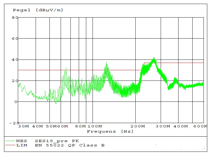
Using a spectrum analyzer to observe the waveform, observe where the problem occurs in the spectrum, which is easy to find the problem
In addition, some low frequency circuit design habits need attention. For example, the conventional single-point grounding is very suitable for low-frequency applications, but it is not suitable for RF signals where there are more EMI problems.
It is believed that some engineers will apply single point grounding to all product designs without recognizing that the use of this grounding method may create more or more complex EMC problems.
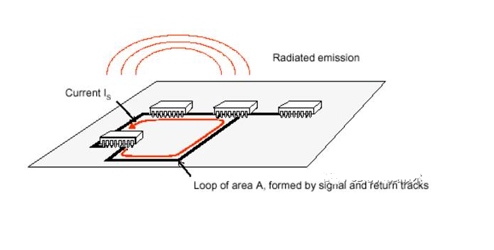
We should also pay attention to the current flow in the circuit components. From circuit knowledge, we know that the current flows from the high voltage to the low voltage, and the current always flows through one or more paths in a closed-loop circuit, so there is a very important rule: design a minimum loop.
For those directions where the interference current is measured, the PCB wiring is modified so that it does not affect the load or sensitive circuit. Applications that require a high impedance path from the power supply to the load must consider all possible paths through which the return current can flow.
We also need to pay attention to PCB wiring. The impedance of a wire or route contains resistance R and inductive reactance. At high frequencies, there is impedance but no capacitive reactance. When the wire frequency is above 100kHz, the wire or wire becomes an inductor. Wires or wires operating above audio may become RF antennas.
In EMC specifications, wires or wires are not allowed to operate below λ/20 of a particular frequency (the antenna is designed to be λ/4 or λ/2 of a particular frequency). If not designed that way, the wiring becomes a highly efficient antenna, making later debugging even trickier.
2. PCB layout
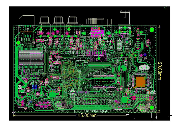
First: Consider the size of the PCB. When the size of PCB is too large, the anti-interference ability of the system decreases and the cost increases with the increase of the wiring, while the size is too small, which easily causes the problem of heat dissipation and mutual interference.
Second: determine the location of special components (such as clock elements) (clock wiring is best not laid around the floor and do not walk around the key signal lines, to avoid interference).
Third: according to the circuit function, the overall layout of PCB. In the component layout, the related components should be as close as possible, so as to obtain a better anti-interference effect.