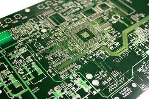
Discussion on PCB electroplating hole filling process
The size of electronic products is becoming thinner and smaller, and directly stacking vias on blind vias is a design method for high-density interconnection. To do a good job of stacking holes, first of all, the flatness of the bottom of the hole should be done well. There are several manufacturing methods, and the electroplating hole filling process is one of the representative ones.
1. Advantages of electroplating and hole filling:
(1) It is conducive to the design of stacked holes and holes on the plate;
(2) Improve electrical performance and help high-frequency design;
(3) helps to dissipate heat;
(4) The plug hole and electrical interconnection are completed in one step;
(5) The blind hole is filled with electroplated copper, which has higher reliability and better conductivity than conductive adhesive
2. Physical influence parameters
Physical parameters that need to be studied include: anode type, distance between cathode and anode, current density, agitation, temperature, rectifier and waveform, etc.
(1) Anode type. When it comes to the type of anode, it is nothing more than a soluble anode and an insoluble anode. Soluble anodes are usually phosphorus-containing copper balls, which are prone to anode mud, pollute the plating solution, and affect the performance of the plating solution. Insoluble anode, good stability, no need for anode maintenance, no anode mud generation, suitable for pulse or DC electroplating; but the consumption of additives is relatively large.
(2) Cathode and anode spacing. The design of the spacing between the cathode and the anode in the electroplating hole filling process is very important, and the design of different types of equipment is also different. No matter how it is designed, it should not violate Farah’s first law.
(3) Stir. There are many types of stirring, including mechanical swing, electric vibration, pneumatic vibration, air stirring, jet flow and so on.
For electroplating hole filling, it is generally preferred to add a jet design based on the configuration of the traditional copper cylinder. The number, spacing and angle of the jets on the jet tube are all factors that have to be considered in the design of the copper cylinder, and a large number of tests must be carried out.
(4) Current density and temperature. Low current density and low temperature can reduce the deposition rate of copper on the surface, while providing enough Cu2 and brightener into the pores. Under this condition, the hole filling ability is enhanced, but the plating efficiency is also reduced.
(5) Rectifier. The rectifier is an important link in the electroplating process. At present, the research on hole filling by electroplating is mostly limited to full-board electroplating. If pattern plating hole filling is considered, the cathode area will become very small. At this time, very high requirements are placed on the output accuracy of the rectifier.The output accuracy of the rectifier should be selected according to the line of the product and the size of the via hole. The thinner the lines and the smaller the holes, the higher the precision requirements for the rectifier should be. Generally, it is advisable to choose a rectifier with an output accuracy within 5%.
(6) Waveform. At present, from the perspective of waveform, there are two types of electroplating and filling holes: pulse electroplating and direct current electroplating. The traditional rectifier is used for direct current plating and hole filling, which is easy to operate, but if the plate is thicker, there is nothing that can be done. PPR rectifier is used for pulse electroplating and hole filling, and there are many operation steps, but it has strong processing ability for thicker boards.
