Disadvantages of PCB traditional four-layer stacking
If the interlayer capacitance is not large enough, the electric field will be distributed over a relatively large area of the board, so that the interlayer impedance is reduced and the return current can flow back to the top layer. In this case, the field generated by this signal may interfere with the field of the nearby changing layer signal. This is not what we had hoped for at all. Unfortunately, on a 4-layer board of 0.062 inches, the layers are far apart and the interlayer capacitance is small
When the wiring changes from layer 1 to Layer 4 or vice versa, then will be lead this problem shown as picture
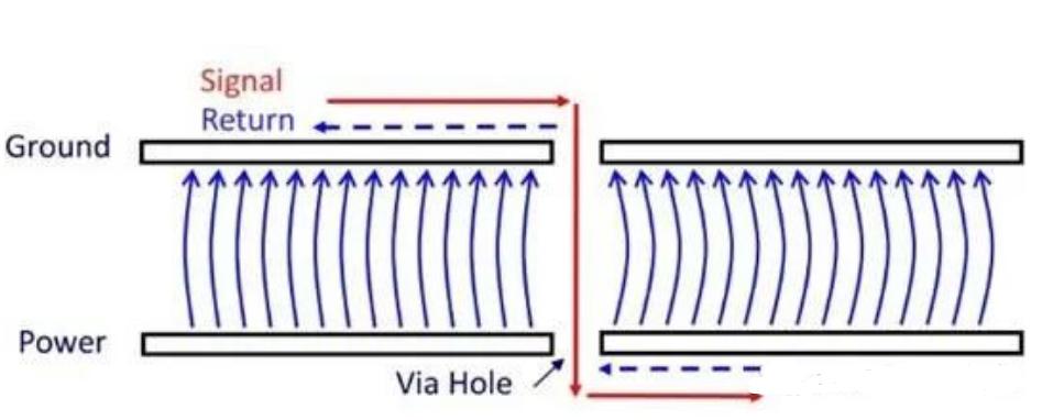
The diagram shows that when the signal tracks from layer 1 to layer 4 (red line), the return current must also change plane (blue line). If the frequency of the signal is high enough and the planes are close together, the return current can flow through the interlayer capacitance that exists between the ground layer and the power layer. However, due to the lack of a direct conductive connection for the return current, the return path is interrupted, and we can think of this interruption as an impedance between planes shown as below picture
If the interlayer capacitance is not large enough, the electric field will be distributed over a relatively large area of the board, so that the interlayer impedance is reduced and the return current can flow back to the top layer. In this case, the field generated by this signal may interfere with the field of the nearby changing layer signal. This is not what we had hoped for at all. Unfortunately, on a 4-layer board of 0.062 inches, the layers are far apart (at least 0.020 inches), and the interlayer capacitance is small. As a result, the electric field interference described above occurs. This may not cause signal integrity issues, but it will certainly create more EMI. This is why, when using the cascade, we avoid changing layers, especially for high frequency signals such as clocks.
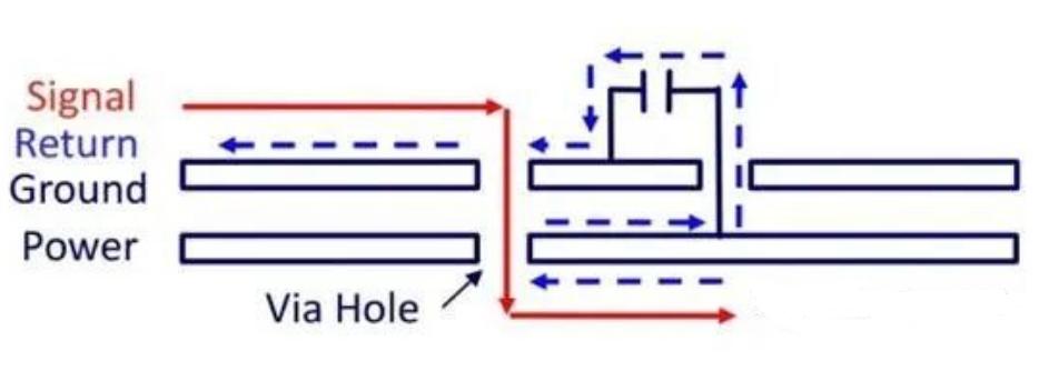
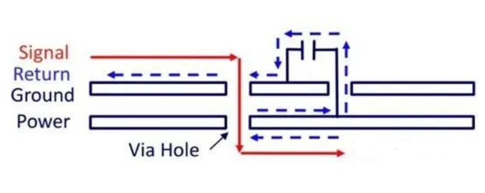
It is common practice to add a decoupling capacitor near the transition pass hole to reduce the impedance experienced by the return current shown as below picture. However, this decoupling capacitor is ineffective for VHF signals due to its low self-resonant frequency. For AC signals with frequencies higher than 200-300 MHz, we cannot rely on decoupling capacitors to create a low-impedance return path. Therefore, we need a decoupling capacitor (for below 200-300 MHz) and a relatively large interboard capacitor for higher frequencies.
This problem can be avoided by not changing the layer of the key signal. However, the small interboard capacitance of the four-layer board leads to another serious problem: power transmission. Clock digital ics typically require large transient power supply currents. As the rise/fall time of IC output decreases, we need to deliver energy at a higher rate. To provide a charge source, we usually place decoupling capacitors very close to each logic IC. However, there is a problem: when we go beyond the self-resonant frequencies, decoupling capacitors cannot efficiently store and transfer energy, because at these frequencies the capacitor will act like an inductor.
Since most ics today have fast rise/fall times (about 500 ps), we need an additional decoupling structure with a higher self-resonant frequency than that of the decoupling capacitor. The interlayer capacitance of a circuit board can be an effective decoupling structure, provided that the layers are close enough to each other to provide sufficient capacitance. Therefore, in addition to the commonly used decoupling capacitors, we prefer to use closely spaced power layers and ground layers to provide transient power to digital ics.
Please note that due to the common circuit board manufacturing process, we usually do not have thin insulators between the second and third layers of the four-layer board. A four-layer board with thin insulators between the second and third layers can cost much more than a conventional four-layer board.